首页>SN74SSQEA32882ZALR>规格书详情
SN74SSQEA32882ZALR集成电路(IC)的专用逻辑器件规格书PDF中文资料

| 厂商型号 |
SN74SSQEA32882ZALR |
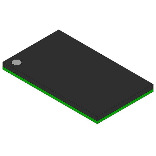
| 参数属性 | SN74SSQEA32882ZALR 封装/外壳为176-TFBGA;包装为卷带(TR)剪切带(CT)Digi-Reel® 得捷定制卷带;类别为集成电路(IC)的专用逻辑器件;产品描述:IC REGSTR BUFFER 28-56BIT 176BGA |
| 功能描述 | 28-Bit to 56-Bit Registered Buffer With Address Parity Test One Pair to Four Pair Differential Clock PLL Driver |
| 丝印标识 | |
| 封装外壳 | NFBGA / 176-TFBGA |
| 文件大小 |
777.11 Kbytes |
| 页面数量 |
13 页 |
| 生产厂商 | Texas Instruments |
| 企业简称 |
TI2【德州仪器】 |
| 中文名称 | 美国德州仪器公司官网 |
| 原厂标识 | TI2 |
| 数据手册 | |
| 更新时间 | 2025-8-3 23:00:00 |
| 人工找货 | SN74SSQEA32882ZALR价格和库存,欢迎联系客服免费人工找货 |
SN74SSQEA32882ZALR规格书详情
SN74SSQEA32882ZALR属于集成电路(IC)的专用逻辑器件。由美国德州仪器公司制造生产的SN74SSQEA32882ZALR专用逻辑器件专用逻辑 IC 设计提供应用特定的逻辑输出类型,例如 BCD 速率倍增、可寻址扫描端口、总线终端阵列、CML 驱动器、比较器、ABT 扫描测试、二进制全加法器、互补对加逆变器、可配置缓冲器、触点颤动消除器、晶体振荡器、延迟元件、差分接收器、LVTTL 到 GTLP 收发器、存储器解码器、电源良好检测器和分频器。
1FEATURES
• JEDEC SSTE32882 Compliant
• 1-to-2 Register Outputs and 1-to-4 Clock Pair
Outputs Support Stacked DDR3 RDIMMs
• CKE Powerdown Mode for Optimized System
Power Consumption
• 1.5V/1.35V Phase Lock Loop Clock Driver for
Buffering One Differential Clock Pair (CK and
CK) and Distributing to Four Differential
Outputs.
• 1.5V/1.35V CMOS Inputs
• Checks Parity on Command and Address
(CS-Gated) Data Inputs
• Configurable Driver Strength
• Uses Internal Feedback Loop
APPLICATIONS
• DDR3 Registered DIMMs up to DDR3-1600
• DDR3L Registered DIMMs up to DDR3L-1333
• Single-, Dual- and Quad-Rank RDIMM
DESCRIPTION
This JEDEC SSTE32882-compliant, 28-bit 1:2 or 26-bit 1:2 and 4-bit 1:1 registering clock driver with parity is
designed for operation on DDR3 registered DIMMs with VDD of 1.5 V and on DDR3L registered DIMMs with VDD
of 1.35 V.
All inputs are 1.5 V and 1.35 V CMOS compatible. All outputs are CMOS drivers optimized to drive DRAM
signals on terminated traces in DDR3 RDIMM applications. The clock outputs Yn and Yn and control net outputs
DxCKEn, DxCSn and DxODTn can be driven with a different strength and skew to optimize signal integrity,
compensate for different loading and equalize signal travel speed.
The SN74SSQEA32882 has two basic modes of operation associated with the Quad Chip Select Enable
(QCSEN) input. When the QCSEN input pin is open (or pulled high), the component has two chip select inputs,
DCS0 and DCS1, and two copies of each chip select output, QACS0, QACS1, QBCS0 and QBCS1. This is the
QuadCS disabled mode. When the QCSEN input pin is pulled low, the component has four chip select inputs
DCS[3:0], and four chip select outputs, QCS[3:0]. This is the QuadCS enabled mode. Through the remainder of
this specification, DCS[n:0] will indicate all of the chip select inputs, where n=1 for QuadCS disabled, and n=3 for
QuadCS enabled. QxCS[n:0] will indicate all of the chip select outputs.
The device also supports a mode where a single device can be mounted on the back side of a DIMM. If
MIRROR=HIGH, Input Bus Termination (IBT) has to stay enabled for all input signals in this case.
The SN74SSQEA32882 operates from a differential clock (CK and CK). Data are registered at the crossing of
CK going HIGH, and CK going LOW. This data could be either re-driven to the outputs or it could be used to
access device internal control registers.
The input bus data integrity is protected by a parity function. All address and command input signals are added
up and the last bit of the sum is compared to the parity signal delivered by the system at the input PAR_IN one
clock cycle later. If they do not match the device pulls the open drain output ERROUT LOW. The control signals
(DCKE0, DCKE1, DODT0, DODT1, DCS[n:0]) are not part of this computation.
The SN74SSQEA32882 implements different power saving mechanisms to reduce thermal power dissipation and
to support system power down states. By disabling unused outputs the power consumption is further reduced.
The package is optimized to support high density DIMMs. By aligning input and output positions towards DIMM
finger signal ordering and SDRAM ballout the device de-scrambles the DIMM traces allowing low cross talk
design with low interconnect latency.
Edge controlled outputs reduce ringing and improve signal eye opening at the SDRAM inputs.
产品属性
更多- 产品编号:
SN74SSQEA32882ZALR
- 制造商:
Texas Instruments
- 类别:
集成电路(IC) > 专用逻辑器件
- 包装:
卷带(TR)剪切带(CT)Digi-Reel® 得捷定制卷带
- 逻辑类型:
1:2 寄存缓冲器,带奇偶位
- 位数:
28,56
- 工作温度:
0°C ~ 85°C
- 安装类型:
表面贴装型
- 封装/外壳:
176-TFBGA
- 供应商器件封装:
176-NFBGA(13.5x8)
- 描述:
IC REGSTR BUFFER 28-56BIT 176BGA
| 供应商 | 型号 | 品牌 | 批号 | 封装 | 库存 | 备注 | 价格 |
|---|---|---|---|---|---|---|---|
TI(德州仪器) |
24+ |
BGA176 |
2317 |
只做原装,提供一站式配单服务,代工代料。BOM配单 |
询价 | ||
TI(德州仪器) |
24+ |
BGA176 |
2886 |
原装现货,免费供样,技术支持,原厂对接 |
询价 | ||
TI |
25+23+ |
NFBGA176 |
31015 |
绝对原装正品全新进口深圳现货 |
询价 | ||
TI |
2025+ |
nFBGA-176 |
16000 |
原装优势绝对有货 |
询价 | ||
TI/德州仪器 |
25+ |
原厂封装 |
10280 |
原厂授权代理,专注军工、汽车、医疗、工业、新能源! |
询价 | ||
TexasInstruments |
18+ |
ICREGSTRBUFFER28-56BIT17 |
6800 |
公司原装现货/欢迎来电咨询! |
询价 | ||
TI |
16+ |
NFBGA |
10000 |
原装正品 |
询价 | ||
Texas Instruments(德州仪器) |
22+ |
NA |
500000 |
万三科技,秉承原装,购芯无忧 |
询价 | ||
TEXAS INSTRUMENTS |
2022+ |
原厂原包装 |
8600 |
全新原装 支持表配单 中国著名电子元器件独立分销 |
询价 | ||
TI |
ROHS+Original |
NA |
894 |
专业电子元器件供应链/QQ 350053121 /正纳电子 |
询价 |

