CDC536DBR集成电路(IC)的时钟发生器PLL频率合成器规格书PDF中文资料
| 厂商型号 |
CDC536DBR |
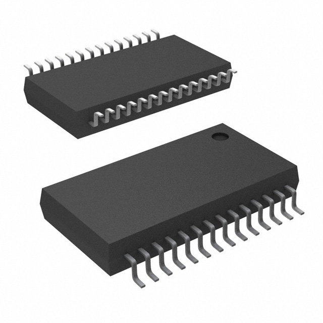
| 参数属性 | CDC536DBR 封装/外壳为28-SSOP(0.209",5.30mm 宽);包装为卷带(TR);类别为集成电路(IC)的时钟发生器PLL频率合成器;产品描述:IC 3.3V PLL CLOCK DRIVER 28-SSOP |
| 功能描述 | 3.3-V PHASE-LOCK LOOP CLOCK DRIVER WITH 3-STATE OUTPUTS |
| 丝印标识 | |
| 封装外壳 | SSOP / 28-SSOP(0.209",5.30mm 宽) |
| 文件大小 |
350.98 Kbytes |
| 页面数量 |
16 页 |
| 生产厂商 | Texas Instruments |
| 企业简称 |
TI2【德州仪器】 |
| 中文名称 | 美国德州仪器公司官网 |
| 原厂标识 |  |
| 数据手册 | |
| 更新时间 | 2025-6-22 22:59:00 |
| 人工找货 | CDC536DBR价格和库存,欢迎联系客服免费人工找货 |
CDC536DBR规格书详情
CDC536DBR属于集成电路(IC)的时钟发生器PLL频率合成器。由美国德州仪器公司制造生产的CDC536DBR时钟发生器,PLL,频率合成器时钟发生器、PLL 和频率合成器集成电路 (IC) 可为逻辑器件提供参考信号的稳定定时脉冲,这些器件包括计算机、微控制器、数据通信系统和图形/视频发生器。这些集成电路可能包括缓冲器、驱动器、分频器、倍频器、多路复用器、合成器、扇出分配器和预分频器。
FEATURES
· Low-Output Skew for Clock-Distribution and
Clock-Generation Applications
· Operates at 3.3-V VCC
· Distributes One Clock Input to Six Outputs
· One Select Input Configures Three Outputs to
Operate at One-Half or Double the Input
Frequency
· No External RC Network Required
· External Feedback Pin (FBIN) Is Used to
Synchronize the Outputs to the Clock Input
· Application for Synchronous DRAM,
High-Speed Microprocessor
· Negative-Edge-Triggered Clear for
Half-Frequency Outputs
· TTL-Compatible Inputs and Outputs
· Outputs Drive 50-W Parallel-Terminated
Transmission Lines
· State-of-the-Art EPIC-IIB™ BiCMOS Design
Significantly Reduces Power Dissipation
· Distributed VCC and Ground Pins Reduce
Switching Noise
· Packaged in Plastic 28-Pin Shrink Small
Outline Package
DESCRIPTION
The CDC536 is a high-performance, low-skew, low-jitter clock driver. It uses a phase-lock loop (PLL) to precisely
align, in both frequency and phase, the clock output signals to the clock input (CLKIN) signal. It is specifically
designed for use with synchronous DRAMs and popular microprocessors operating at speeds from 50 MHz to
100 MHz or down to 25 MHz on outputs configured as half-frequency outputs. The CDC536 operates at 3.3-V
VCC and is designed to drive a 50-W transmission line.
The feedback input (FBIN) is used to synchronize the output clocks in frequency and phase to the input clock
(CLKIN). One of the six output clocks must be fed back to FBIN for the PLL to maintain synchronization between
CLKIN and the outputs. The output used as the feedback pin is synchronized to the same frequency as CLKIN.
The Y outputs can be configured to switch in phase and at the same frequency as CLKIN. The select (SEL) input
configures three Y outputs to operate at one-half or double the CLKIN frequency depending on which pin is fed
back to FBIN (see Tables 1 and 2). All output signal duty cycles are adjusted to 50% independent of the duty
cycle at the input clock.
Output-enable (OE) is provided for output control. When OE is high, the outputs are in the high-impedance state.
When OE is low, the outputs are active. TEST is used for factory testing of the device and can be use to bypass
the PLL. TEST should be strapped to GND for normal operation.
产品属性
更多- 产品编号:
CDC536DBR
- 制造商:
Texas Instruments
- 类别:
集成电路(IC) > 时钟发生器,PLL,频率合成器
- 包装:
卷带(TR)
- 类型:
PLL 时钟驱动器
- PLL:
带旁路
- 输入:
TTL
- 输出:
LVTTL
- 比率 - 输入:
1:6
- 差分 - 输入:
无/无
- 频率 - 最大值:
100MHz
- 分频器/倍频器:
是/是
- 电压 - 供电:
3V ~ 3.6V
- 工作温度:
0°C ~ 70°C
- 安装类型:
表面贴装型
- 封装/外壳:
28-SSOP(0.209",5.30mm 宽)
- 供应商器件封装:
28-SSOP
- 描述:
IC 3.3V PLL CLOCK DRIVER 28-SSOP
| 供应商 | 型号 | 品牌 | 批号 | 封装 | 库存 | 备注 | 价格 |
|---|---|---|---|---|---|---|---|
TI(德州仪器) |
24+ |
SSOP28208mil |
2317 |
只做原装,提供一站式配单服务,代工代料。BOM配单 |
询价 | ||
TI/德州仪器 |
24+ |
NA/ |
15 |
优势代理渠道,原装正品,可全系列订货开增值税票 |
询价 | ||
TI/德州仪器 |
25+ |
SSOP-28 |
860000 |
明嘉莱只做原装正品现货 |
询价 | ||
TI/德州仪器 |
2023+ |
SSOP28 |
6895 |
原厂全新正品旗舰店优势现货 |
询价 | ||
TI |
25+ |
SSOP28 |
15 |
原装正品,假一罚十! |
询价 | ||
TI |
25+23+ |
SSOP28 |
32010 |
绝对原装正品全新进口深圳现货 |
询价 | ||
TI(德州仪器) |
2024+ |
SSOP-28-208mil |
500000 |
诚信服务,绝对原装原盘 |
询价 | ||
Texas |
25+ |
25000 |
原厂原包 深圳现货 主打品牌 假一赔百 可开票! |
询价 | |||
TI |
24+ |
SSOP28 |
1800 |
询价 | |||
TI |
2025+ |
SSOP-28 |
16000 |
原装优势绝对有货 |
询价 |