首页>74AUP2T1326GF>规格书详情
74AUP2T1326GF集成电路(IC)缓冲器驱动器接收器收发器规格书PDF中文资料
| 厂商型号 |
74AUP2T1326GF |
| 参数属性 | 74AUP2T1326GF 封装/外壳为10-XFDFN;包装为管件;类别为集成电路(IC) > 缓冲器,驱动器,接收器,收发器;产品描述:IC BUFFER NON-INVERT 3.6V 10XSON |
| 功能描述 | Low-power dual supply buffer/line driver; 3-state |
| 文件大小 |
801.31 Kbytes |
| 页面数量 |
17 页 |
| 生产厂商 | Nexperia B.V. All rights reserved |
| 企业简称 |
NEXPERIA【安世】 |
| 中文名称 | 安世半导体(中国)有限公司官网 |
| 原厂标识 |  |
| 数据手册 | |
| 更新时间 | 2024-5-17 18:26:00 |
74AUP2T1326GF规格书详情
1. General description
The 74AUP2T1326 is a high-performance, dual supply, low-power, low-voltage, dual
buffer/line driver with output enable circuitry.
The 74AUP2T1326 is designed for logic-level translation and combines the functions of
the 74AUP1G32 and 74AUP2G126. The buffer/line driver is controlled by two output
enable inputs (1OE and 2OE). A logic LOW on input 1OE causes the output 2Y to assume
a high-impedance OFF-state, a logic LOW on 2OE causes the output 3Y to assume a
high-impedance OFF-state. The output 1Y is the result of a logic OR of the two output
enable inputs.
The output enable inputs (1OE and 2OE) are Schmitt trigger inputs, they switch at
different voltages for positive and negative-going signals. The difference between the
positive voltage VT+ and the negative voltage VT is defined as the input hysteresis
voltage VH. The output enable inputs accept standard input signals and are capable of
transforming slowly changing input signals into sharply defined, jitter-free output signals
Both VCC(A) and VCC(B) can be supplied at any voltage between 1.1 V and 3.6 V making
the device suitable for interfacing between any of the low voltage nodes (1.2 V, 1.5 V,
1.8 V, 2.5 V and 3.3 V) with compatible input levels. Pins 1OE, 2OE and 1Y are
referenced to VCC(A) and pins A, 2Y and 3Y are referenced to VCC(B).
The device ensures low static and dynamic power consumption and is fully specified for
partial power down applications using IOFF. The IOFF circuitry disables the outputs,
preventing any damaging backflow current through the device when it is powered down.
2. Features and benefits
Wide supply voltage range:
VCC(A): 1.1 V to 3.6 V; VCC(B): 1.1 V to 3.6 V.
High noise immunity
Complies with JEDEC standards:
JESD8-7 (1.2 V to 1.95 V)
JESD8-5 (1.8 V to 2.7 V)
JESD8-B (2.7 V to 3.6 V)
ESD protection:
HBM JESD22-A114F Class 2A exceeds 2000 V
MM JESD22-A115-A exceeds 200 V
CDM JESD22-C101E exceeds 1000 V
Low static power consumption; ICC = 0.9 A (maximum)
Latch-up performance exceeds 100 mA per JESD 78 Class II
Inputs accept voltages up to 3.6 V
Low noise overshoot and undershoot < 10 of VCC
IOFF circuitry provides partial Power-down mode operation
Multiple package options
Specified from 40 C to +85 C
74AUP2T1326GF属于集成电路(IC) > 缓冲器,驱动器,接收器,收发器。安世半导体(中国)有限公司制造生产的74AUP2T1326GF缓冲器,驱动器,接收器,收发器逻辑缓冲器、驱动器、接收器和收发器允许隔离对某个电路的逻辑信号的访问,以用于另一电路。缓冲器将其输入信号(不变或反相)传递到其输出,并可能用于清除弱信号或驱动负载。在布尔逻辑仿真器中,缓冲器主要用于增加传播延迟。逻辑接收器和收发器允许在数据总线之间进行隔离通信。
产品属性
- 产品编号:
74AUP2T1326GF,132
- 制造商:
Nexperia USA Inc.
- 类别:
集成电路(IC) > 缓冲器,驱动器,接收器,收发器
- 系列:
74AUP
- 包装:
管件
- 逻辑类型:
缓冲器,非反向
- 每个元件位数:
1
- 输出类型:
三态
- 电流 - 输出高、低:
4mA,4mA
- 电压 - 供电:
1.1V ~ 3.6V
- 工作温度:
-40°C ~ 85°C(TA)
- 安装类型:
表面贴装型
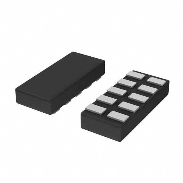
- 封装/外壳:
10-XFDFN
- 供应商器件封装:
10-XSON(1.7x1)
- 描述:
IC BUFFER NON-INVERT 3.6V 10XSON
| 供应商 | 型号 | 品牌 | 批号 | 封装 | 库存 | 备注 | 价格 |
|---|---|---|---|---|---|---|---|
NXP(恩智浦) |
23+ |
VSSOP8 |
6000 |
询价 | |||
Nexperia(安世) |
2021+ |
XSON-10 |
499 |
询价 | |||
Nexperia(安世) |
23+ |
XSON10(1x1 |
5001 |
原装现货,免费供样,技术支持,原厂对接 |
询价 | ||
Nexperia(安世) |
23+ |
XSON10(1x1.7) |
7350 |
现货供应,当天可交货!免费送样,原厂技术支持!!! |
询价 | ||
Nexperia(安世) |
1923+ |
VSSOP-8 |
2260 |
向鸿只做原装正品,我们没有假货!仓库库存优势 |
询价 | ||
Nexperia(安世) |
22+ |
XSON-10 |
9852 |
只做原装正品现货,或订货假一赔十! |
询价 | ||
Nexperia USA Inc. |
21+ |
8-VFSOP(0.091,2.30mm 宽) |
15000 |
正规渠道/品质保证/原装正品现货 |
询价 | ||
NP2 |
2147+ |
原厂封装 |
12500 |
原厂原装现货,订货价格优势,终端BOM表可配单提供样 |
询价 | ||
NXP-恩智浦 |
24+25+/26+27+ |
逻辑计算IC |
36218 |
一一有问必回一特殊渠道一有长期订货一备货HK仓库 |
询价 | ||
NP2 |
2305+ |
原厂封装 |
12500 |
15年芯片行业经验/只供原装正品:0755-83267371邹小姐 |
询价 |