MPC860DE集成电路(IC)微处理器规格书PDF中文资料
| 厂商型号 |
MPC860DE |
| 参数属性 | MPC860DE 封装/外壳为357-BBGA;包装为托盘;类别为集成电路(IC) > 微处理器;产品描述:IC MPU MPC8XX 66MHZ 357BGA |
| 功能描述 | MPC860 PowerQUICC Family Hardware Specifications |
| 文件大小 |
1.05548 Mbytes |
| 页面数量 |
77 页 |
| 生产厂商 | NXP Semiconductors |
| 企业简称 |
nxp【恩智浦】 |
| 中文名称 | 恩智浦半导体公司官网 |
| 原厂标识 |  |
| 数据手册 | |
| 更新时间 | 2024-6-13 0:03:00 |
MPC860DE规格书详情
This hardware specification contains detailed information on
power considerations, DC/AC electrical characteristics, and
AC timing specifications for the MPC860 family.
To locate published errata or updates for this document, see
the MPC860 product summary page on the website listed on
the back cover of this document or contact your local
Freescale sales office.
2 Features
The following list summarizes the key MPC860 features:
• Embedded single-issue, 32-bit core (implementing the Power Architecture technology) with
thirty-two 32-bit general-purpose registers (GPRs)
— The core performs branch prediction with conditional prefetch without conditional execution.
— 4- or 8-Kbyte data cache and 4- or 16-Kbyte instruction cache (see Table 1)
– 16-Kbyte instruction caches are four-way, set-associative with 256 sets; 4-Kbyte instruction
caches are two-way, set-associative with 128 sets.
– 8-Kbyte data caches are two-way, set-associative with 256 sets; 4-Kbyte data caches are
two-way, set-associative with 128 sets.
– Cache coherency for both instruction and data caches is maintained on 128-bit (4-word)
cache blocks.
– Caches are physically addressed, implement a least recently used (LRU) replacement
algorithm, and are lockable on a cache block basis.
— MMUs with 32-entry TLB, fully-associative instruction, and data TLBs
— MMUs support multiple page sizes of 4-, 16-, and 512-Kbytes, and 8-Mbytes; 16 virtual
address spaces and 16 protection groups
— Advanced on-chip-emulation debug mode
• Up to 32-bit data bus (dynamic bus sizing for 8, 16, and 32 bits)
• 32 address lines
• Operates at up to 80 MHz
• Memory controller (eight banks)
— Contains complete dynamic RAM (DRAM) controller
— Each bank can be a chip select or RAS to support a DRAM bank.
— Up to 15 wait states programmable per memory bank
— Glueless interface to DRAM, SIMMS, SRAM, EPROM, Flash EPROM, and other memory
devices
— DRAM controller programmable to support most size and speed memory interfaces
— Four CAS lines, four WE lines, and one OE line
— Boot chip-select available at reset (options for 8-, 16-, or 32-bit memory)
— Variable block sizes (32 Kbytes to 256 Mbytes)
— Selectable write protection
— On-chip bus arbitration logic
• General-purpose timers
— Four 16-bit timers or two 32-bit timers
— Gate mode can enable/disable counting
— Interrupt can be masked on reference match and event capture.
• System integration unit (SIU)
— Bus monitor
— Software watchdog
— Periodic interrupt timer (PIT)
— Low-power stop mode
— Clock synthesizer
— Decrementer, time base, and real-time clock (RTC)
— Reset controller
— IEEE 1149.1™ Std. test access port (JTAG)
• Interrupts
— Seven external interrupt request (IRQ) lines
— 12 port pins with interrupt capability
— 23 internal interrupt sources
— Programmable priority between SCCs
— Programmable highest priority request
• 10/100 Mbps Ethernet support, fully compliant with the IEEE 802.3u® Standard (not available
when using ATM over UTOPIA interface)
• ATM support compliant with ATM forum UNI 4.0 specification
— Cell processing up to 50–70 Mbps at 50-MHz system clock
— Cell multiplexing/demultiplexing
— Support of AAL5 and AAL0 protocols on a per-VC basis. AAL0 support enables OAM and
software implementation of other protocols.
— ATM pace control (APC) scheduler, providing direct support for constant bit rate (CBR) and
unspecified bit rate (UBR) and providing control mechanisms enabling software support of
available bit rate (ABR)
— Physical interface support for UTOPIA (10/100-Mbps is not supported with this interface) and
byte-aligned serial (for example, T1/E1/ADSL)
— UTOPIA-mode ATM supports level-1 master with cell-level handshake, multi-PHY (up to four
physical layer devices), connection to 25-, 51-, or 155-Mbps framers, and UTOPIA/system
clock ratios of 1/2 or 1/3.
— Serial-mode ATM connection supports transmission convergence (TC) function for
T1/E1/ADSL lines, cell delineation, cell payload scrambling/descrambling, automatic
idle/unassigned cell insertion/stripping, header error control (HEC) generation, checking, and
statistics.
• Communications processor module (CPM)
— RISC communications processor (CP)
— Communication-specific commands (for example, GRACEFUL STOP TRANSMIT, ENTER HUNT
MODE, and RESTART TRANSMIT)
— Supports continuous mode transmission and reception on all serial channels
— Up to 8 Kbytes of dual-port RAM
— 16 serial DMA (SDMA) channels
— Three parallel I/O registers with open-drain capability
• Four baud-rate generators (BRGs)
— Independent (can be tied to any SCC or SMC)
— Allows changes during operation
— Autobaud support option
• Four serial communications controllers (SCCs)
— Ethernet/IEEE 802.3® standard optional on SCC1–4, supporting full 10-Mbps operation
(available only on specially programmed devices)
— HDLC/SDLC (all channels supported at 2 Mbps)
— HDLC bus (implements an HDLC-based local area network (LAN))
— Asynchronous HDLC to support point-to-point protocol (PPP)
— AppleTalk
— Universal asynchronous receiver transmitter (UART)
— Synchronous UART
— Serial infrared (IrDA)
— Binary synchronous communication (BISYNC)
— Totally transparent (bit streams)
— Totally transparent (frame-based with optional cyclic redundancy check (CRC))
• Two SMCs (serial management channels)
— UART
— Transparent
— General circuit interface (GCI) controller
— Can be connected to the time-division multiplexed (TDM) channels
• One SPI (serial peripheral interface)
— Supports master and slave modes
— Supports multimaster operation on the same bus
• One I2C (inter-integrated circuit) port
— Supports master and slave modes
— Multiple-master environment support
• Time-slot assigner (TSA)
— Allows SCCs and SMCs to run in multiplexed and/or non-multiplexed operation
— Supports T1, CEPT, PCM highway, ISDN basic rate, ISDN primary rate, user defined
— 1- or 8-bit resolution
— Allows independent transmit and receive routing, frame synchronization, and clocking
— Allows dynamic changes
— Can be internally connected to six serial channels (four SCCs and two SMCs)
• Parallel interface port (PIP)
— Centronics interface support
— Supports fast connection between compatible ports on the MPC860 or the MC68360
• PCMCIA interface
— Master (socket) interface, release 2.1 compliant
— Supports two independent PCMCIA sockets
— Supports eight memory or I/O windows
• Low power support
— Full on—all units fully powered
— Doze—core functional units disabled except time base decrementer, PLL, memory controller,
RTC, and CPM in low-power standby
— Sleep—all units disabled except RTC and PIT, PLL active for fast wake up
— Deep sleep—all units disabled including PLL except RTC and PIT
— Power down mode—all units powered down except PLL, RTC, PIT, time base, and
decrementer
• Debug interface
— Eight comparators: four operate on instruction address, two operate on data address, and two
operate on data
— Supports conditions: = ≠
— Each watchpoint can generate a break-point internally.
• 3.3-V operation with 5-V TTL compatibility except EXTAL and EXTCLK
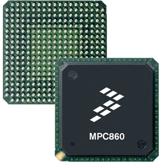
• 357-pin ball grid array (BGA) package
MPC860DE属于集成电路(IC) > 微处理器。恩智浦半导体公司制造生产的MPC860DE微处理器微处理器产品是用于信息和数据处理的集成电路。与主要按照制造商所选术语而视为微控制器的类似产品相比,这些器件有所不同。但是按照传统,微处理器不会在设备内集成工作存储器,不太可能集成混合信号外设,并且可能在更为复杂的软件范式下使用,这些范式涉及使用操作系统来管理多任务同时执行。
产品属性
- 产品编号:
MPC860DECVR66D4
- 制造商:
NXP USA Inc.
- 类别:
集成电路(IC) > 微处理器
- 系列:
MPC8xx
- 包装:
托盘
- 核心处理器:
MPC8xx
- 内核数/总线宽度:
1 核,32 位
- 速度:
66MHz
- 协处理器/DSP:
通信;CPM
- RAM 控制器:
DRAM
- 图形加速:
无
- 以太网:
10Mbps(2)
- 电压 - I/O:
3.3V
- 工作温度:
-40°C ~ 95°C(TA)
- 封装/外壳:
357-BBGA
- 供应商器件封装:
357-PBGA(25x25)
- 描述:
IC MPU MPC8XX 66MHZ 357BGA
| 供应商 | 型号 | 品牌 | 批号 | 封装 | 库存 | 备注 | 价格 |
|---|---|---|---|---|---|---|---|
FREESCALE |
14+ |
BGA |
15 |
一级代理,专注军工、汽车、医疗、工业、新能源、电力 |
询价 | ||
NXP/恩智浦 |
2020+ |
NA |
80000 |
只做自己库存,全新原装进口正品假一赔百,可开13%增 |
询价 | ||
Freescale(飞思卡尔) |
2022+ |
60000 |
原厂原装,假一罚十 |
询价 | |||
FREESCALE |
22+ |
BGA |
100000 |
代理渠道/只做原装/可含税 |
询价 | ||
Freescale(飞思卡尔) |
23+ |
NA/ |
8735 |
原厂直销,现货供应,账期支持! |
询价 | ||
NXP |
23+ |
357PBGA |
4568 |
原厂原装正品现货,代理渠道,支持订货!!! |
询价 | ||
FREESCALE |
2018+ |
BGA |
30617 |
专营FREESCALE品牌全新原装热卖 |
询价 | ||
FREESCALE |
21+ |
BGA357 |
1709 |
询价 | |||
FREESCALE |
1836+ |
BGA |
9852 |
只做原装正品现货!或订货假一赔十! |
询价 | ||
FREESCALE |
22+ |
BGA |
354000 |
询价 |