8T49N285集成电路(IC)时钟发生器PLL频率合成器规格书PDF中文资料
| 厂商型号 |
8T49N285 |
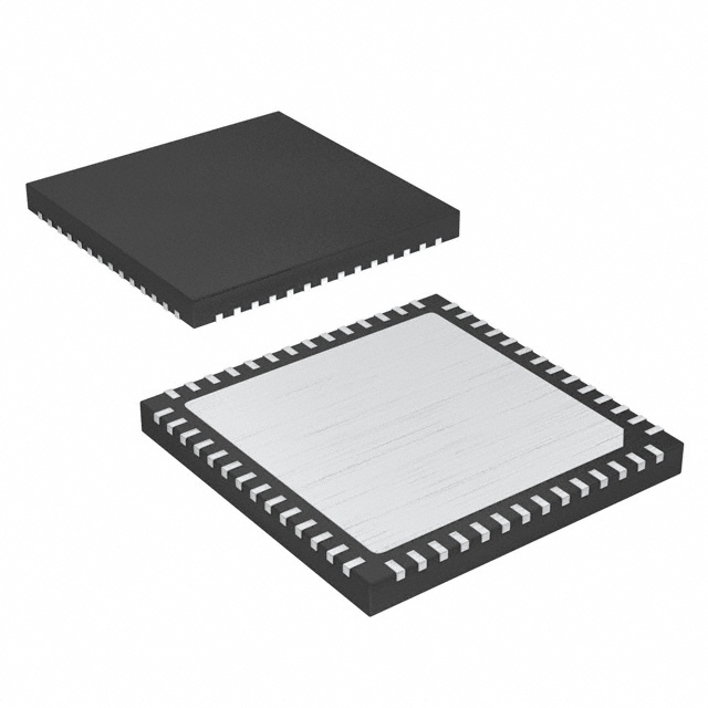
| 参数属性 | 8T49N285 封装/外壳为56-VFQFN 裸露焊盘;包装为托盘;类别为集成电路(IC) > 时钟发生器,PLL,频率合成器;产品描述:IC TRANSLATOR UNIV FREQ VFQFN |
| 功能描述 | FemtoClock® NG Octal Universal Frequency Translator |
| 文件大小 |
1.26772 Mbytes |
| 页面数量 |
68 页 |
| 生产厂商 | Renesas Electronics America |
| 企业简称 |
RENESAS【瑞萨】 |
| 中文名称 | 瑞萨科技有限公司官网 |
| 原厂标识 |  |
| 数据手册 | |
| 更新时间 | 2024-6-17 18:46:00 |
相关芯片规格书
更多8T49N285规格书详情
Description
The 8T49N285 has a fractional-feedback PLL that can be used as a
jitter attenuator or frequency translator. It is equipped with six integer
and two fractional output dividers, allowing the generation of up to 8
different output frequencies, ranging from 8kHz to 1GHz. Three of
these frequencies are completely independent of each other and the
inputs. The other five are related frequencies. The eight outputs may
select among LVPECL, LVDS, HCSL or LVCMOS output levels.
This functionality makes it ideal to be used in any frequency
translation application, including 1G, 10G, 40G, and 100G
Synchronous Ethernet, OTN, and SONET/SDH, including ITU-T
G.709 (2009) FEC rates. The device may also behave as a frequency
synthesizer.
The 8T49N285 accepts up to two differential or single-ended input
clocks and a crystal input. The PLL can lock to either input clock, but
both input clocks must be related in frequency.
The device supports hitless reference switching between input
clocks. The device monitors both input clocks for Loss of Signal
(LOS). It generates an alarm when an input clock failure is detected.
Automatic and manual hitless reference switching options are
supported. LOS behavior can be set to support gapped or un-gapped
clocks.
The 8T49N285 supports holdover with an initial accuracy of ±50ppB
from the point where the loss of all applicable input reference(s) has
been detected. It maintains a historical average operating point that
may be returned to in holdover at a limited phase slope.
The device places no constraints on input to output frequency
conversion, supporting all FEC rates, including the new revision of
ITU-T Recommendation G.709 (2009), most with 0ppm conversion
error.
The PLL has a register-selectable loop bandwidth from 1.4Hz to
360Hz.
Each output supports individual phase delay settings to allow
output-output alignment.
The device supports Output Enable inputs and Lock, Holdover and
LOS status outputs.
The device is programmable through an I2C interface. It also supports
I
2C master capability to allow the register configuration to be read
from an external EEPROM.
Features
• Supports SDH/SONET and Synchronous Ethernet clocks
including all FEC rate conversions
• <0.3ps RMS typical jitter (including spurs),12kHz to 20MHz
• Operating modes: locked to input signal, holdover and free-run
• Initial holdover accuracy of ±50ppb
• Accepts two LVPECL, LVDS, LVHSTL, HCSL or LVCMOS
input clocks
• Accepts frequencies ranging from 8kHz up to 875MHz
• Auto and manual input clock selection with hitless switching
• Clock input monitoring, including support for gapped clocks
• Phase-Slope Limiting and Fully Hitless Switching options to
control output phase transients
• Operates from a 10MHz to 40MHz fundamental-mode crystal
• Generates 8 LVPECL/LVDS/HCSL or 16 LVCMOS output clocks
• Output frequencies ranging from 8kHz up to 1.0GHz (diff)
• Output frequencies ranging from 8kHz to 250MHz (LVCMOS)
• Four General Purpose I/O pins with optional support for status &
control:
• Four Output Enable control inputs may be mapped to any of the
eight outputs
• Lock, Holdover & Loss-of-Signal status outputs
• Open-drain Interrupt pin
• Nine programmable PLL loop bandwidth settings from 1.4Hz to
360Hz.
• Optional Fast Lock function
• Programmable output phase delays in steps as small as 16ps
• Register programmable through I2C or via external I2C EEPROM
• Bypass clock paths for system tests
• Power supply modes
VCC / VCCA / VCCO
3.3V / 3.3V / 3.3V
3.3V / 3.3V / 2.5V
3.3V / 3.3V / 1.8V (LVCMOS)
2.5V / 2.5V / 3.3V
2.5V / 2.5V / 2.5V
2.5V / 2.5V / 1.8V (LVCMOS)
• -40°C to 85°C ambient operating temperature
• Package: 56QFN, lead-free RoHs (6)
8T49N285属于集成电路(IC) > 时钟发生器,PLL,频率合成器。瑞萨科技有限公司制造生产的8T49N285时钟发生器,PLL,频率合成器时钟发生器、PLL 和频率合成器集成电路 (IC) 可为逻辑器件提供参考信号的稳定定时脉冲,这些器件包括计算机、微控制器、数据通信系统和图形/视频发生器。这些集成电路可能包括缓冲器、驱动器、分频器、倍频器、多路复用器、合成器、扇出分配器和预分频器。
产品属性
- 产品编号:
8T49N285-999NLGI
- 制造商:
Renesas Electronics America Inc
- 类别:
集成电路(IC) > 时钟发生器,PLL,频率合成器
- 系列:
FemtoClock® NG
- 包装:
托盘
- PLL:
带旁路
- 输入:
HCSL,LVCMOS,LVDSM,LVHSTL,LVPECL,晶体
- 输出:
HSCL,LVCMOS,LVDS,LVPECL
- 比率 - 输入:
3:8
- 差分 - 输入:
是/是
- 频率 - 最大值:
1GHz
- 分频器/倍频器:
是/无
- 电压 - 供电:
2.375V ~ 3.465V
- 工作温度:
-40°C ~ 85°C
- 安装类型:
表面贴装型
- 封装/外壳:
56-VFQFN 裸露焊盘
- 供应商器件封装:
56-VFQFPN(8x8)
- 描述:
IC TRANSLATOR UNIV FREQ VFQFN
| 供应商 | 型号 | 品牌 | 批号 | 封装 | 库存 | 备注 | 价格 |
|---|---|---|---|---|---|---|---|
RENESAS |
22+ |
NA |
2655 |
原装正品支持实单 |
询价 | ||
RENESAS |
23+ |
NA |
6000 |
全新、原装 |
询价 | ||
RENESAS(瑞萨)/IDT |
23+ |
VFQFPN56(8x8) |
6000 |
诚信服务,绝对原装原盘 |
询价 | ||
IDT |
1931+ |
N/A |
1186 |
加我qq或微信,了解更多详细信息,体验一站式购物 |
询价 | ||
IDT |
22+ |
NA |
267 |
加我QQ或微信咨询更多详细信息, |
询价 | ||
IDT/RENESAS |
22+ |
NA |
24500 |
瑞萨全系列在售 |
询价 | ||
IDT |
1744+ |
VQFN56 |
5 |
一级代理,专注军工、汽车、医疗、工业、新能源、电力 |
询价 | ||
IDT(Renesas收购) |
23+ |
NA/ |
8735 |
原厂直销,现货供应,账期支持! |
询价 | ||
Renesas/IDT |
23+/24+ |
BGA-324 |
15000 |
原装进口、正品保障、合作持久 |
询价 | ||
RENESAS/瑞萨 |
24+23+ |
12580 |
16年现货库存供应商终端BOM表可配单提供样品 |
询价 |
相关库存
更多- 8T49N282C-DDDNLGI8
- 8T49N283
- 8T49N283C-DDDNLGI
- 8T49N283C-DDDNLGI8
- 8T49N282C-DDDNLGI#
- 8T49N283C-DDDNLGI#
- 8T49N281C-DDDNLGI#
- 8T49N285A-007NLGI
- 8T49N285A-999NLGI
- 8T49N285A-002NLGI8
- 8T49N285A-002NLGI
- 8T49N285A-000NLGI8
- 8T49N285A-006NLGI
- 8T49N285A-001NLGI8
- 8T49N285A-001NLGI
- 8T49N285A-007NLGI8
- 8T49N285_16
- 8T49N285A-006NLGI8
- 8T49N285A-000NLGI
- 8T49N285A-999NLGI8
- 8T49N285_18
- 8T49N285A-DDDNLGI
- 8T49N285A-DDDNLGI8